Liquid Crystal Solar Panel Technology

Typical Mono And Polycrystalline Silicon Solar Cells Top And Download Scientific Diagram
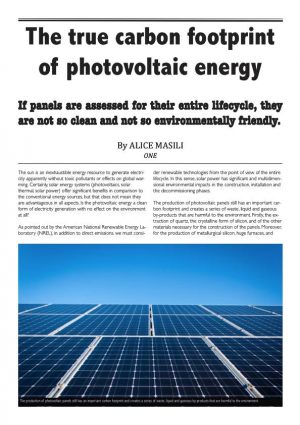
The True Carbon Footprint Of Photovoltaic Energy One Only Natural Energy
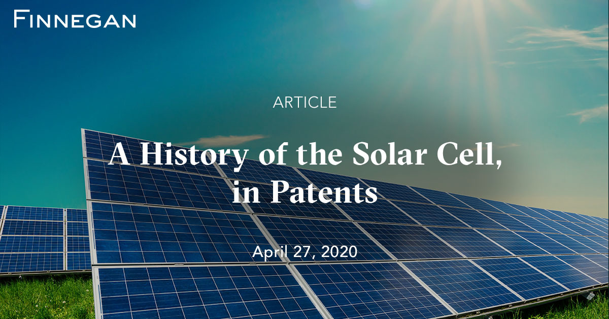
A History Of The Solar Cell In Patents Articles Finnegan Leading Intellectual Property Law Firm
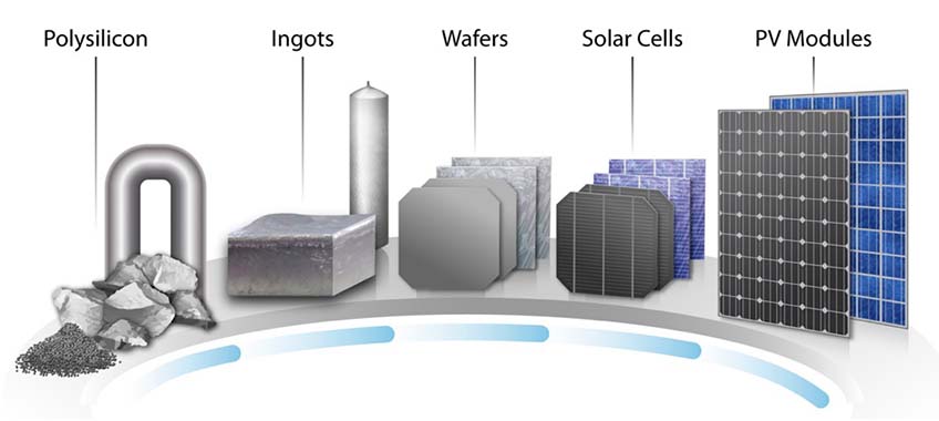
Solar Technology Cost Analysis Energy Analysis Nrel

Production Of Liquid Solar Fuels And Their Use In Fuel Cells Sciencedirect

Usc Develops Printable Liquid Solar Cells For Flexible Low Cost Panels Solar Energy Diy Solar Energy Panels Solar Energy
Furnace for the activation of cdte solar cells.
Liquid crystal solar panel technology.

Liquid Crystal Display Lcd A Type Of Flat Panel Display That Uses An Array Of Backlit Thin Film Transisto Liquid Crystal Display Lcd Panel Design Transistors

What Is An Lcd Liquid Crystal Display Https Www Xenarc Com Lcd Technology Html Xenarc Technologies Is A Rugged Lcd M Liquid Crystal Display Technology Lcd

Global Polysilicon Panel Market Research Report 2019 With Images Mini Solar Panel Paneling Solar Module

Ted Lee Bavin A Worker Walks Through The Installed Solar Modules At The Naini Solar Power Plant In The Northern Indi Solar Pool Solar Panels Outdoor Solutions
Https Www Mdpi Com 2076 3417 10 7 2337 Pdf

Could This Fill The Funding Gaps That Prevent Startups From Getting To Market Solarpanels Solarenergy Sola With Images Green Energy Sustainable Energy Alternative Energy

Solar Lights Don T Charge Anymore Try This To Rejuvenate The Lights Solar Power House Solar Power Diy Diy Solar Panel

Dye Sensitized Solar Cell Wikipedia

The Best Solar Panel In India Solarmyplace In 2020 Solar Panels Portable Solar Panels Solar

World Of Science How A Solar Photovoltaic Cell Works Photovoltaic Cells Solar Thermal Solar Heating

Dual Axis Solar Tracker With Online Energy Monitor Solar Tracker Solar Panels Solar Energy Panels

Active Matrix Liquid Crystal Displays Lcd Liquid Crystal Display Electronic Engineering Lcd
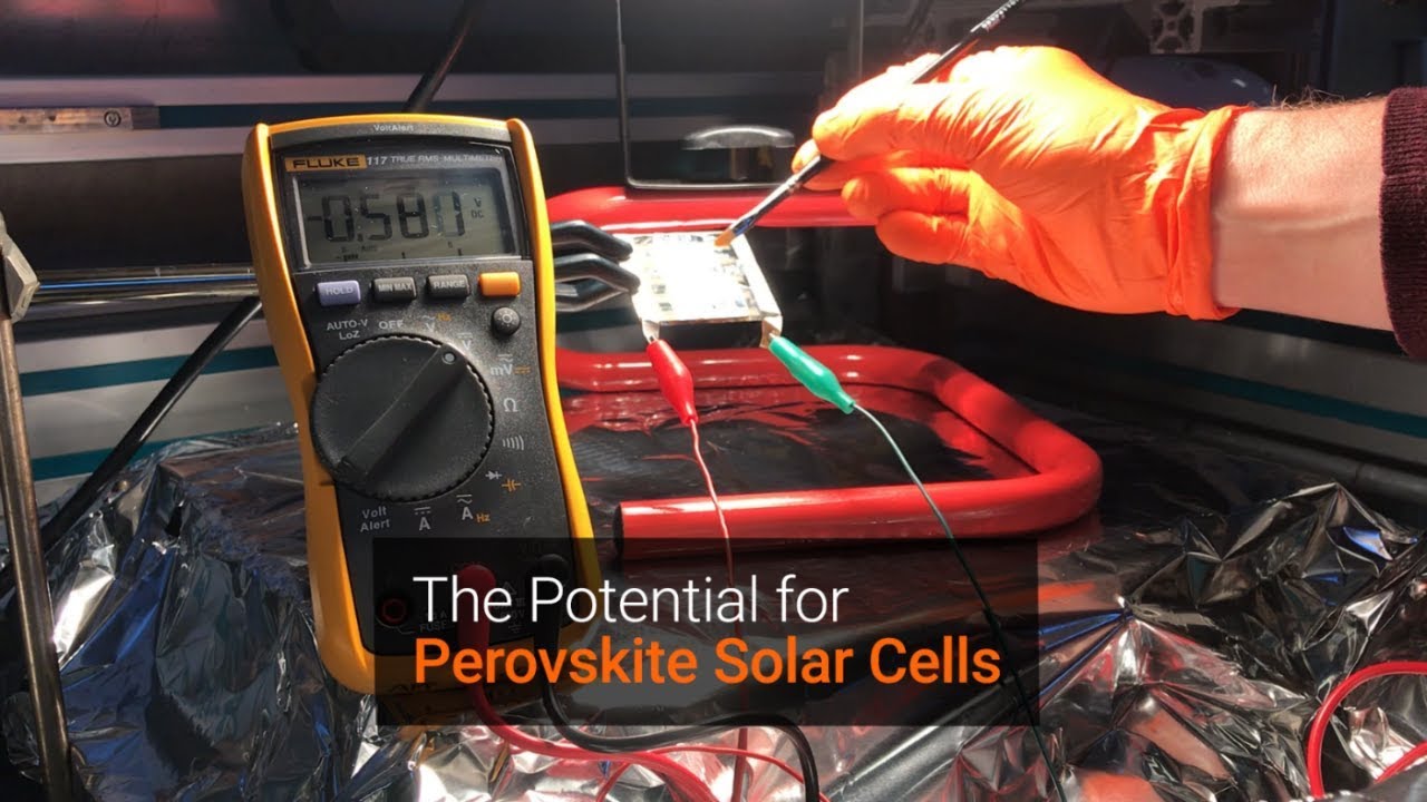
Perovskite Solar Cells Department Of Energy
3 Chapter 3 Solar Energy

Solar Power Diy Solar Power Training Pv Photovoltaic Harbor Freight Free Energy Photovoltaic Kits Solar Panels Solar Energy Panels Best Solar Panels

Lubi Solar Pump Contact Us Today 91 079 66745300 Solar Solar Power Panels Solar Panels

Green Energy For All Solar Energy Feed In Tariff Deciding To Go Environmentally Friendly By Converting To Solar Power House Solar Power Panels Solar Panels

Solar Power Technical Tips And Nice To Know Information Northern Arizona Wind Sun
1

Mesquite Solar 1 Power Plant Arizona Power Technology Energy News And Market Analysis

Grid Tie Solar Systems With Battery Backup Solar Panels Solar Panel Installation Paneling

Diy Solar Panels Diy Solar Panel Diy Solar Solar Energy Panels

Integrated Inverter Control Machine Solar Power Inverter Liquid Crystal Display Power Inverters

Click Visit Link Above For More Info Panneau Photovoltaique Energie Solaire Solaire Diy
Source : pinterest.com
